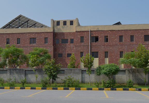
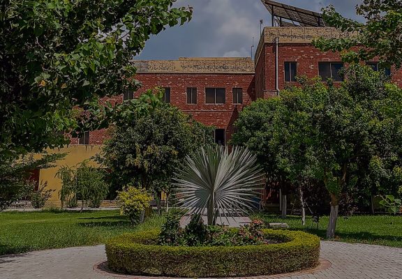
MEMS / Chip Design Group
Ten 15 MS level scholarships (uptoRs 20,000 per month) for full-time students are available to work on the development of MEMS Gyroscope and accelerometer for Satellite, Mineral Exploration, and Automobile applications
We are a group of Nerds who are doing research for fun to develop something useful to bring comfort in our lives by developing MEMS-based sensors and solutions of the size of the diameter hair. MEMS are very small-scale devices that are of the size of a micrometer (1 million times smaller than a meter). These magical and nonvisible MEMS devices are everywhere around you from airplane to, car to a mobile phone.
Mission
The lab has developed skilled manpower through scientific research to produce world-class MEMS (Microelectromechanical Systems) and microchip design experts having expertise in design, fabrication, and testing to produce world-class R&D in MEMS/Chip development and initiate commercial activities in this area in Pakistan while supporting the local needs of the academic institutions and strategic organizations.
Lab also aims to develop artificial intelligence-based MEMS Inertial Navigation Systems (gyroscope, accelerometers, magnetometer) for mobile robots and other applications.
Objective
- Develop MEMS and IC (Integrated Chip) Design, Prototyping, and Testing skills through R&D
- Design and Fabrication of Microgrippers for Molecule Inspection and cell manipulation, Gyroscope, and accelerometer for inertia applications
- Design and Fabrication of path planning for autonomous cars using a Gyroscope and accelerometer with Artificial Intelligence and Machine learning capabilities.
- Produce highly skilled manpower at Undergraduate and graduate levels that can take research and development leading jobs in Pakistan and abroad.
- Provide MEMS design, prototyping, and testing consulting at national and international levels
We are a group of Nerds who are doing research for fun to develop something useful to bring comfort in our lives by developing MEMS-based sensors and solutions of the size of the diameter hair. MEMS are very small-scale devices that are of the size of a micrometer (1 million times smaller than a meter). These magical and nonvisible MEMS devices are everywhere around you from airplane to, car to a mobile phone.
Projects
IMU-based Gesture Controlled Mobile Robot:
We have implemented a system-level application through which the user can give commands to wireless robots using gestures based on motion capture sensors mounted on the human hands and joints. Through this method the user can control or navigate the robot by using the gestures of the hand, thereby interacting with the robotic system. The command signals are tracked using the motion sensors. The gestures provide a rich and intuitive form of interaction for controlling robots. Application areas are Medical Surgery, Surveillance Robots, Motion Capture Tools
Implementation of Inertial navigation system for Autonomous Path Planning of Mobile Robot:
We have implemented a system-level application through which a robot can navigate autonomously from a starting point to an endpoint, the on-board integrated controller creates the necessary trajectories that will drive the robot. The on-board Inertial sensors measure the motion parameters of the robot and the controller estimates the position, velocity, heading, and orientation of the robot. The onboard controller also implements steering correction in case of deviation from its reference heading. Application areas are Autonomous Robots, Autonomous Cars, Surveillance Robots, Guidance Systems, and Navigation Systems.
Fundings (Past)
- Ignite Technology Fund, 2008, 2012, 2015, Rs 40 Million
- HEC, 2007, 2008, 5 Million
- NESCOM, 2012, 0.5 Million
Software Facilities
- Intelligence
- MEMSPro
Publications
65 Research Publications in International Journals and Conferences
Collaborations
- Queen University, Kingston, Canada
- Air University, Islamabad
- EME College, Rawalpindi
- First MEMS Design Startup in Progress
Hardware Facilities
- Robotics Platforms
- Microsystem Analyzer Shaker
- High voltage Amplifiers
- Probe Station
- Signal Generators
MEMS Chips Developed
Academics contribute specialist courses in power systems and broad power engineering areas of electrical engineering-based specializations.
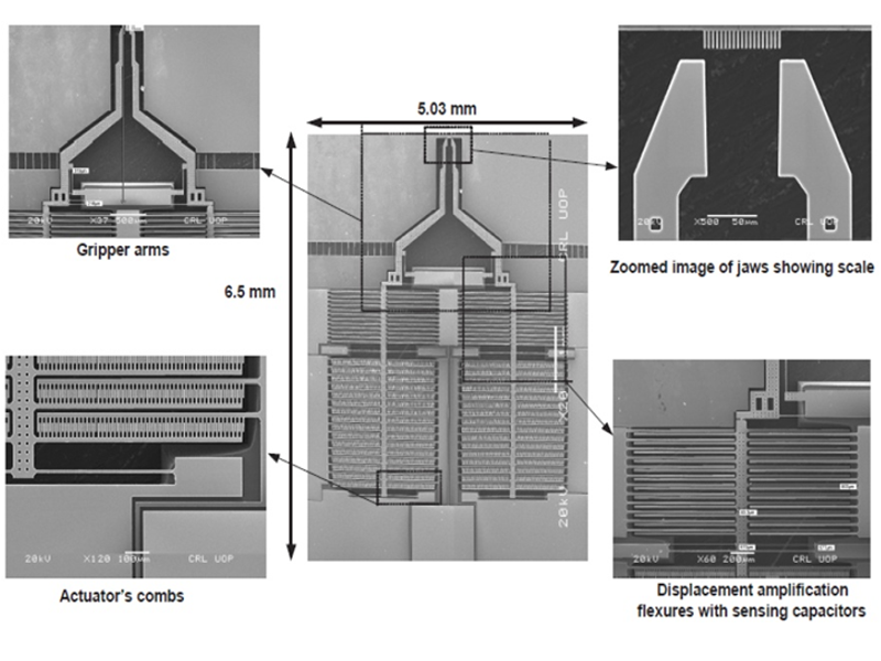
Microgripper to Hold Blood Cells
[7] Shaffat A. Bazaz, Fahimullah Khan, Rana Iqtidar Shakoor ”Design, simulation and testing of electrostatic SOI MUMPS based microgripper integrated with contact sensor”, Sensors and Actuators: A. Physical (Elsevier),vol. 167, 2011. [8] Fahimullah Khan , S.A Bazaz, Muhammad Sohail ” Design and implementation of Electrostatic SOI-MUMPs microgripper” Journal of Microsystem Technologies.
3-Axis MEMS Accelerometer
A 3-Axis MEMS Accelerometer is a small, microelectromechanical sensor that measures acceleration along three perpendicular axes, enabling motion detection and orientation tracking.
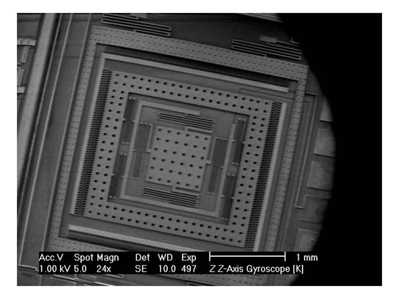
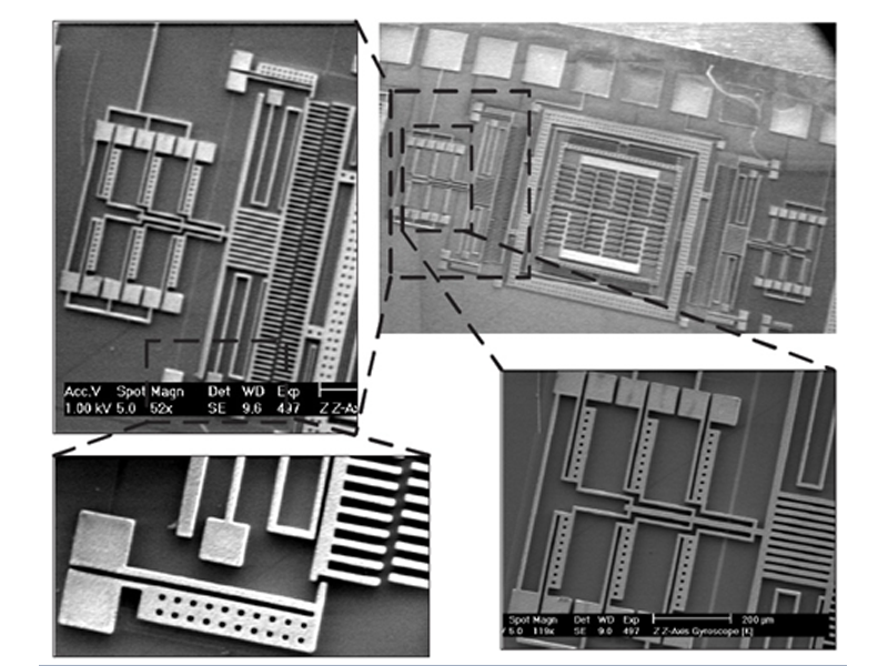
Development of MEMS Gyroscope: 3rd Generation
Performance Enhancement through Micro Locking Mechanism
Thermal MEMS Gyroscope
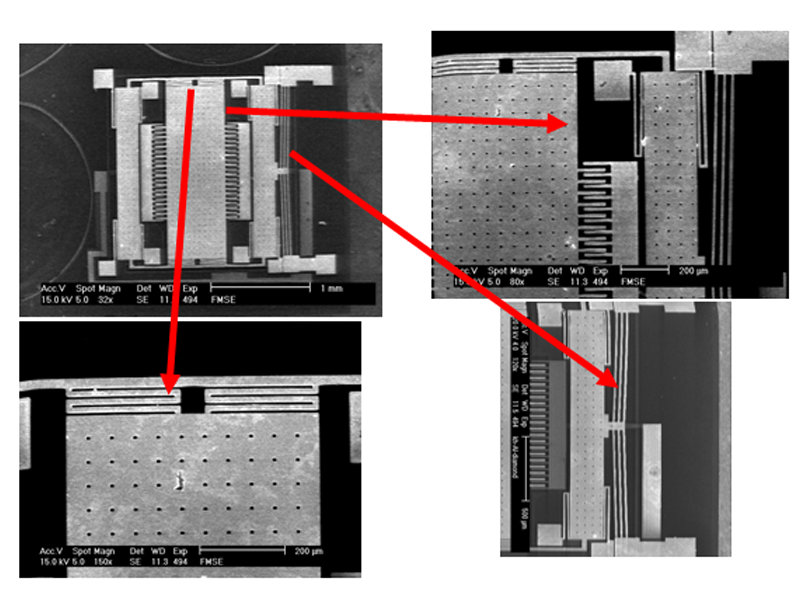
Scanning Electron Microscope pictures of Thermal Micro-Gyroscope developed at CASE [8] Fahimullah Khan , S.A Bazaz, Muhammad Sohail ” Design and implementation of Electrostatic SOI-MUMPs microgripper” Journal of Microsystem Technologies.
Fabrication
We are in the process of establishing a MEMS fabrication facility to offer custom process solutions to meet the requirement of academic researchers and industrial customers. Our facilities include a class 100/1000 clean room environment having the following process capabilities.
Photolithography
- Photolithography of 1µm feature on 6” (150mm) wafers
- Single or double-sided alignment
- Spin & Spray resist coating
Wet Etching
- Anisotropic silicon etching
- Metal etching
- Oxide & Nitride etching
Deposition
- Silicon oxides & nitrides by PECVD
- PVD sputtering of metals, oxides & nitrides
- Oxides or nitrides by reactive sputtering
- LPCVD of SiO2 and Si3N4
- Dry and wet oxidation
- Atmospheric annealing
Reactive Ion Etching
- Deep reactive etching of silicon (DRIE)
- ICP etching of silicon oxide & nitride
Ion Implantation
- Ion implantation of B, P & As @ 200KeV
- Rapid thermal annealing
Metrology and characterization
- Film thickness measurement
- Resistivity four point probe
- Thin film stress measurement
- Ellipsometer
- Optical profiler
- IR microscope
- Optical measuring microscope
- Probe station with parametric analyzer
Dicing & packaging
- Wafer bonder (fusion & anodic)
- Dicing of silicon & glass wafers
- Wire bonder
- Plasma treatment system

